|
|
|
Who's Online
There currently are 5944 guests online. |
|
Categories
|
|
Information
|
|
Featured Product
|
|
|
 |
|
|
There are currently no product reviews.
 ;
This manual is accurate and of high quality. It is only volume 2 of the service manual. This is schematic, parts lists, and exploded mechanical drawings. The theory of operation and the diss-assembly instructions are in volume 1. The unit can be tricky to dis-assemble portions of so the volume 1 manual can be important. The product description of the manual is accurate but it does not say anything about volume 1 and the image of the front page does clearly say Volume 2.
 ;
Wellll again thank you very much fast and effective. Clear and well done for such an old TV!!!!
;
It has all the information you will need to fix it. The main circuit diagram is only A4 but being a PDF, you can print it to any size - I did it on two sheets of A3 and it didnt lose any detail - just made it readable when pinned up above the bench. I've found the fault, just need to buy some obscure bits to get it going again!
I cant fault the process, I paid for the manual in the morning and it was ready to download by lunch time.
;
Very good copy in a 54 pages PDF archive. This is my sixth purchase here. :)
;
Another excellent buy! File too clear and explanatory.
IC DESCRIPTION IC, LA9241ML
Pin No. 1 2 3 4 5 6 7 8 9 10 11 12 13 14 15 16 17 Pin Name FIN2 FIN1 E F TB TETE TESI SCI TH TA TDTD JP TO FD FDI/O I I I I I I O I I I O I I I O O I Description Pin to which external pickup photo diode is connected. RF signal is created by adding with the FIN1 pin signal. FE signal is created by subtracting from the FIN1 pin signal. Pin to which external pickup photo diode is connected. Pin to which external pickup photo diode is connected. TE signal is created by subtracting from the F pin signal. Pin to which external pickup photo diode is connected. DC component of the TE signal is input. Pin to which external resistor setting the TE signal gain is connected between the TE pin. TE signal output pin. TES �Track Error Sense� comparator input pin. TE signal is passed through a bandpass filter then input. Shock detection signal input pin. Tracking gain time constant setting pin. TA amplifier output pin. Pin to which external tracking phase compensation constants are connected between the TD and VR pins. Tracking phase compensation setting pin. Tracking jump signal (kick pulse) amplitude setting pin. Tracking control signal output pin. Focusing control signal output pin. Pin to which external focusing phase compensation constants are connected between the FD and FA pins. 18 FA I Pin to which external focusing phase compensation constants are connected between the FD� and FA� pins. 19 20 21 22 23 24 25 26 27 28 29 30, 31 32, 33 34 35 FAFE FEAGND SP SPI SPG SPSPD SLEQ SLD SL-, SL+ JP-, JP+ TGL TOFF I O I � O I I I O I O I I I I Pin to which external focusing phase compensation constants are connected between the FA and FE pins. FE signal output pin. Pin to which external FE signal gain setting resistor is connected between the FE pin. Analog signal GND. Signal ended output of the CV+and CV- pin input signal. Spndle amp input. Pin to which external spindle gain setting resistor in 12 cm mode is connected. Pin to which external spindle phase compensation constants are connected together with SPD pin. Spindle control signal output pin. Pin to which external sled phase compensation constants are connected. Sled control signal output pin. Sled advance signal input pin from microprocessor. Tracking jump signal input pin from DSP. Tracking gain control signal input from DSP. Low gain when TGL = H. Tracking off control signal input pin from DSP. Off when TOFF = H.
29
 $4.99 CSDTD53 AIWA
Owner's Manual Complete owner's manual in digital format. The manual will be available for download as PDF file aft… 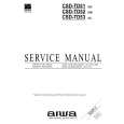 $4.99 CSD-TD53 AIWA
Parts Catalog Parts Catalog only. It's available in PDF format. Useful, if Your equipment is broken and You need t…
|
|
|
> |
|